
HBM’s Share of Global DRAM Capacity Exceeds 20% for the First Time in 2026
In 2026 the semiconductor industry recorded a milestone: high-bandwidth memory (HBM) has crossed the 20% threshold of global DRAM wafer-equivalent capacity for the first time. This is not merely a metric—it's a structural signal. It reflects changing customer priorities, deliberate capital allocation decisions by leading memory makers, and maturation of advanced packaging ecosystems that finally translate wafer output into finished, high-value modules at scale.
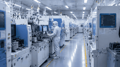
Context: why this percentage matters
DRAM capacity is traditionally measured in wafer-equivalents because wafers are the primary industrial unit for production planning and capital investment. A 20% share for HBM indicates that one-fifth of the global investment and production effort in DRAM technology now targets stacked, high-bandwidth formats rather than commodity DDR parts. That has several consequences:
- System architecture: Designers can plan for more on-package high-bandwidth memory availability, changing the trade-offs between bandwidth, latency, and cost for accelerators and servers.
- Supplier economics: Memory vendors with HBM capability now influence overall DRAM pricing dynamics since a non-trivial share of capacity is tied to strategic, contracted demand rather than spot commodity purchases.
- Packaging and OSAT demand: Finished-module output depends heavily on packaging; a larger wafer share for HBM amplifies demand for interposers, hybrid bonding, and advanced assembly services.
The rest of this post explores how the industry reached this inflection point and why it matters for customers, suppliers, and investors.
Drivers that pushed HBM to 20%
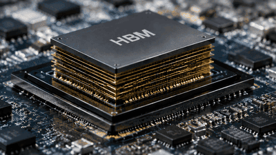
Multiple converging factors created the HBM capacity expansion of 2024–2026. Key drivers include:
- Explosive AI demand: Large language models, foundation models, and inference fleets require memory bandwidth at scales that traditional DIMM-based approaches struggle to provide. HBM’s superior bandwidth-per-watt makes it the preferred option for top-tier accelerators.
- Economic signaling from hyperscalers: Major cloud providers committed to multi-year capacity reservations and co-investments, de-risking capex for memory makers and encouraging re-allocation of fab capacity from commodity DRAM to HBM-capable processes.
- Packaging maturity: Advances in hybrid bonding, CoWoS-style interposers, microfluidic cooling prototypes, and improved OSAT yield engineering made it possible to convert wafer output into finished HBM modules at higher throughput.
- Product roadmaps and process convergence: DRAM process nodes evolved to support higher die capacities and stackability with acceptable yields, making it economically viable to dedicate more wafers to HBM die production.
- Strategic corporate choices: SK Hynix, Samsung, and Micron prioritized HBM investments as part of multi-year strategies, shifting a larger share of their DRAM-capable wafer starts toward HBM designs and packaging integrations.
These drivers combined to create a durable demand profile and a willingness among suppliers to redirect capacity in favor of higher-margin, strategic HBM products.
How capacity was reallocated and expanded
Reaching a 20% share required both building new capacity and reallocating existing lines. The main mechanisms were:
- Process conversion: Foundries and IDMs repurposed certain DRAM process lines for HBM die variants, using minor reticle and process tweaks to support larger die and TSV or hybrid-bond architectures.
- New fab investments: Select memory makers announced and brought online new capacity targeted at HBM die production to meet contract-backed demand.
- Packaging expansion: OSATs and integrated memory vendors invested in hybrid-bond tooling, fine-pitch metrology, and interposer supply to ensure finished-module throughput matched wafer output.
- Co-investment deals: Several hyperscalers provided prepayments or capacity commitments in exchange for prioritized allocation, effectively underwriting parts of the capex required for HBM growth.
Importantly, wafer allocation numbers understate the difficulty of delivering finished HBM stacks. Packaging yield and test throughput are the gating steps; the industry synchronized investments across wafer fabs and packaging to avoid wafer inventories that could not be fulfilled as modules.
Regional footprint and geopolitical implications
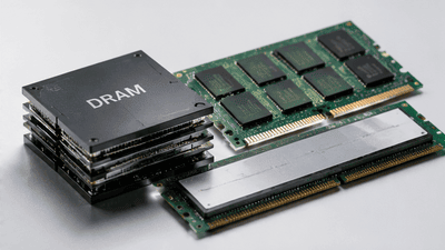
The HBM capacity expansion has a distinct regional profile that interacts with geopolitics and industrial policy:
- South Korea: SK Hynix and Samsung expanded HBM wafer and packaging capacity in Korea, benefiting from deep local supply chains and government support for advanced packaging ecosystems.
- United States: Micron’s U.S. investments and targeted onshore packaging projects aimed to meet hyperscaler and defense-oriented demand that prefers domestically sourced critical components.
- Taiwan and Southeast Asia: These regions scaled OSAT and test-and-pack operations, providing the assembly bandwidth needed to convert wafer output into finished modules.
- China: Local demand remains strong, but export controls and trade restrictions on certain advanced packaging tools limited how much of the newest HBM capacity could physically be built or used for the highest-performance modules intended for global hyperscalers.
Policymakers and companies responded by increasing diversification—building redundant OSAT and interposer capacity across allied regions and signing cross-border agreements to ensure continuity of supply for critical customers.
Impact on pricing and margins
An immediate question when supply shifts toward high-end product is: what happens to prices and margin pools? The 2026 outcome shows nuanced dynamics:
- HBM ASPs remain elevated relative to commodity DRAM: System-level demand and limited initial packaging capacity kept premiums intact for HBM modules, especially HBM3e and HBM4 variants.
- Commodity DRAM price stabilization: With a non-trivial share of wafers diverted to HBM, commodity DRAM supply tightened modestly, supporting higher DDR ASPs than would have occurred otherwise during the same period.
- Gross-margin uplift for HBM producers: Memory makers with integrated packaging captured higher value per wafer-equivalent as they sold finished modules instead of wafer-only die, improving blended gross margins.
- Packaging premium and OSAT pricing power: Short-term scarcity of hybrid-bond-capable lines gave OSATs with those skills pricing power, though new capacity commitments began to dampen that effect toward late 2026.
Overall, the shift improved supplier margins while introducing a new layer of pricing complexity tied to packaging throughput and system-level demand curves.
Effects on system design and OEM strategies
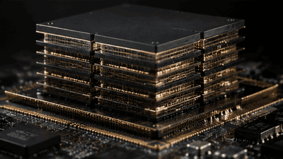
Given more abundant HBM availability, system architects and OEMs adapted design choices and procurement strategies:
- Design-for-HBM became more common: Where previously HBM was reserved for top-tier accelerators, more designs now assume accessible HBM capacity, enabling denser, more power-efficient servers and appliances.
- Qualification and multi-sourcing: OEMs invested in qualifying multiple HBM suppliers early to ensure flexibility and reduce the risk of supplier-specific shortages.
- Alternative architectures explored: Increased HBM availability encouraged hybrid memory architectures in which HBM acts as the performance tier and DDR remains bulk capacity, simplifying software tiers and memory management.
- Long-term contracting: Many OEMs negotiated multi-year supply deals to secure priority access during future spikes and to stabilize procurement pricing for large cloud deployments.
These changes reduce the premium-per-unit cost when amortized at the system level, since better performance-per-watt and reduced networking overhead often lower total cost of ownership for large deployments.
Supply-chain winners and losers
The shift to >20% HBM capacity redistributed value across the supply chain. Winners include:
- Integrated memory makers with packaging capability: These companies captured wafer and module margins and benefited from premium product pricing.
- OSATs specialized in hybrid bonding and fine-pitch assembly: Early investments and strong process IP paid off during the capacity ramp.
- Equipment vendors for hybrid bonding, metrology, and advanced CMP: High demand for precision tooling accelerated sales and long lead times for these suppliers.
- Materials suppliers of advanced underfills, thermally conductive films, and activation chemistries: Recurring consumable demand scaled rapidly with packaging throughput.
Losers or stressed parties included players with heavy exposure to commodity DRAM who lacked an HBM strategy and small OSATs unable to invest in hybrid-bond tooling quickly. The sudden reallocation of wafer capacity also created transitional dislocations: some commodity-focused fabs faced underutilization while the market rebalanced.
Operational challenges encountered during the ramp
Scaling HBM to a fifth of global DRAM capacity was not without operational pain. Notable challenges were:
- Packaging bottlenecks: Even with packaging investments, throughput lagged wafer supply initially, creating unfinished inventory and pressuring working capital.
- Yield learning: Hybrid bonding and high-die-count stacks required aggressive yield-engineering programs; initial defect rates increased COGS until improvements took hold.
- Logistics and test capacity: Test time per module increased due to more complex qualification; test-house capacity had to be expanded rapidly.
- Coordination across suppliers: Siloed investments resulted in mismatched ramp rates; companies mitigated this by forming cross-company co-investment agreements and supply guarantees.
Addressing these challenges required operational discipline, capital spending prioritization, and tight partnerships between memory makers, OSATs, and OEMs.
Market and technological implications going forward
Crossing the 20% threshold has longer-term implications for where compute innovation will focus and how memory evolution will proceed:
- HBM becomes a standard design lever: Architects will increasingly assume HBM capability in high-performance designs, accelerating software and hardware co-optimization for bandwidth-rich memory hierarchies.
- Shift in R&D priorities: Memory vendors will allocate more R&D to HBM variants (HBM4 and beyond), packaging innovations, and thermal solutions, potentially slowing commodity DRAM feature churn.
- Secondary markets grow: Refurbishment, module-level testing, and packaging improvement services gain traction as demand for qualified HBM modules rises.
- Potential for consolidation: OSATs and interposer fabs with early expertise may consolidate value; smaller players may seek partnerships or acquisition to survive.
The industry may also see more creative system-level memory constructs—multiple smaller HBM chips across modular packages, disaggregated memory pools connected by advanced interconnects, and hybrid memory fabrics that blur the line between on-package and off-package memory tiers.
Risks and watchpoints
While the 20% milestone marks progress, several risks could alter the trajectory:
- Overinvestment and oversupply: If many suppliers expand simultaneously without matching system-level demand growth, HBM ASPs could fall, compressing margins.
- Technological substitutes: Breakthroughs in alternative memory technologies or monolithic 3D DRAM could change the value proposition of HBM.
- Geopolitical disruption: Export controls on advanced packaging tools or sanctions could limit where top-end HBM modules are produced or sold.
- Macro slowdown in AI capex: A significant, prolonged pause in hyperscaler spending on AI training infrastructure would reduce near-term HBM uptake.
Industry participants and investors should monitor capacity announcements, packaging throughput, backlog metrics, and hyperscaler procurement plans to gauge whether the 20% share is a new baseline or an over-stretched peak.
Practical recommendations for stakeholders
Given the new capacity mix, different stakeholders should consider targeted actions:
- Memory makers: Maintain a balanced portfolio, secure packaging capacity, and protect margins by capturing module-level value through integration or preferred OSAT partnerships.
- OSATs and interposer fabs: Accelerate yield engineering and offer co-development programs to become strategic partners for memory vendors and OEMs.
- OEMs and hyperscalers: Lock in multi-year supply where density matters, co-design thermal and mechanical interfaces early, and qualify multiple suppliers to avoid allocation risks.
- Investors: Watch capex pacing, packaging throughput, and long-term contracts; favor firms showing disciplined allocation that aligns wafer starts with packaging and test capacity.
- Policymakers: Encourage regional packaging capability and workforce development to reduce single-point risks in critical compute supply chains.
Conclusion
HBM exceeding 20% of global DRAM wafer-equivalent capacity in 2026 is a structural turning point. It reflects a realignment of industry priorities toward performance-per-watt and bandwidth-centric system design, driven by AI and HPC demand and enabled by coordinated investments across wafers, interposers, and packaging. The milestone improves margin profiles for vertically integrated suppliers, raises the strategic importance of OSAT and interposer capacity, and changes procurement and system-design norms for OEMs and hyperscalers.
Whether 20% becomes the new floor or a temporary peak depends on execution: yield improvements, packaging throughput, and steady demand growth from AI workloads. For now, the milestone signals a maturing ecosystem where HBM is no longer a niche premium but a mainstream element of high-performance compute design—and where supply-chain orchestration determines who captures the most value from this important transition.
You May Like

Narrowing Spread Between NAND Spot and Contract Prices in 2026 – A Signal
By 2026, one of the most watched metrics in the NAND flash market has started to shift in a subtle but meaningful way: the spread between spot prices and long‑term contract prices is narrowing. For casual observers, this may look like just another incremental change in a notoriously volatile industry. For memory makers, module houses, device OEMs, and data center buyers, however, a tightening gap between spot and contract prices is a signal—a reflection of evolving supply–demand balance, risk perceptions, and strategic behavior on both sides of the market.

Price Divergence Trading Strategies Between NAND Flash and DRAM ETFs
NAND flash and DRAM sit at the core of AI storage and computing power. Both are memory, but they are not the same business. DRAM is main memory—fast, volatile, and central to high‑bandwidth workloads like AI training and inference. NAND is non‑volatile storage—slower than DRAM, but crucial to persistent data and large‑scale object storage. The cycles that drive their pricing and margins overlap, yet they often diverge. That divergence is where trading strategies between NAND and DRAM ETFs become interesting.

China’s HBM Localization Progress: The Catch-Up Pace of CXMT and XMC
China’s drive to localize advanced memory technologies has accelerated over the past several years. High-Bandwidth Memory (HBM) sits near the center of that strategy because it is integral to AI accelerators, high-performance computing (HPC) and other strategic compute platforms. Two domestic players—ChangXin Memory Technologies (CXMT) and XMC (Xianghui Memory, commonly referred to as XMC)—have become focal points in assessing how quickly China can close the gap with international incumbents on HBM die, stacking, and packaging.

Thermal Simulation Challenges and Solutions in 3DIC AI Chip Design
As AI workloads push chips to deliver ever higher compute density, designers are increasingly turning to three‑dimensional integration (3DIC) to stack dies vertically and pack more functionality into limited footprints. While 3DIC architectures unlock significant performance and bandwidth advantages, they also introduce complex thermal behaviors that are far harder to predict and manage than in traditional 2D layouts.

An Attempt at Compiling a Memory+Compute Fusion Thematic Index – A Dual-Track Framework
Most AI investors talk about “compute” as if it were the whole story: GPUs, accelerators, chips, cores. But every one of those cores needs somewhere to read from and write to. Memory and storage define how wide the data highway really is. In practice, AI performance is a fusion of compute and memory, not a solo act. So why do so many indices and ETFs separate them into different silos—one for semiconductors, one for memory, one for data centers—when the actual workloads keep blending them?
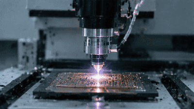
Surging Demand for Laser Drilling and Plasma Dicing Equipment in Advanced Packaging
Advanced packaging has become one of the semiconductor industry’s most important growth engines, and it is now pulling a surprising set of process tools into the spotlight. Among the most in-demand are laser drilling and plasma dicing equipment. These machines sit close to the heart of heterogeneous integration, fan-out packaging, wafer thinning, TSV formation, glass substrate processing, and other advanced flows where precision, yield, and throughput matter enormously. As packaging moves from a back-end afterthought to a strategic platform, the equipment used to shape, open, and separate materials has become just as important as the dies themselves.

D2D Interface Bandwidth and Latency Comparison in Chiplet Architectures
Chiplet architecture has turned the package into a real performance battleground. Once multiple dies are placed side by side or stacked within the same advanced package, the quality of the die-to-die, or D2D, interface becomes one of the most important determinants of system behavior. Bandwidth is no longer a nice-to-have metric, and latency is no longer a small implementation detail. Together, they shape whether a chiplet system feels nearly monolithic or frustratingly fragmented.

Stock Selection Logic and Alpha Validation of ESG-Themed Semi ETFs
Semiconductor themed ETFs are no longer just about growth and cycles. A growing subset now layers environmental, social, and governance (ESG) criteria on top of traditional sector exposure. These ESG semi ETFs promise two things at once: access to one of the market’s most powerful secular themes, and alignment with sustainability and governance standards. The pitch is appealing, but it raises two hard questions. First, how exactly are these stocks being selected? Second, does the ESG overlay help, hurt, or leave alpha unchanged?